A working mental model of GPU hardware for ML engineers who use these chips daily but have never traced what happens below the CUDA API

Generating a single token from a 70 billion parameter model on an H100 requires reading roughly 140 GB of weights from memory and performing about 140 billion arithmetic operations on them. That works out to one operation per byte loaded. Memory bandwidth, not compute throughput, determines how fast that token comes out. By the end of this series, the reasoning that leads from the hardware specs to this conclusion will be derivable from first principles, and the architectural responses to it, KV cache management, quantization, and prefill-decode disaggregation, will follow as direct consequences.
Part one builds the hardware mental model. How a GPU is constructed at the silicon level, how the SIMT execution model organizes thousands of threads into warps, and how the six-tier memory hierarchy moves data toward those threads. Part two uses this foundation to introduce arithmetic intensity, the roofline model, and the LLM-specific consequences.
Table of Contents
- Why GPUs Are Built the Way They Are
- How Work Gets Organized
- Where Data Lives
- Where This Goes Next
1. Why GPUs Are Built the Way They Are
A CPU core can finish a single instruction in roughly one nanosecond. A GPU thread is, by most reasonable measures, slower than that. What a GPU has is twenty thousand of them running at once, and the architecture is built around extracting throughput from that population.

1.1 The throughput-latency tradeoff
CPUs optimize for finishing one task quickly. GPUs optimize for finishing many tasks at once, even when each individual task is slow. The split is a consequence of a fixed transistor budget being spent in two different directions. Chip designers choose where the silicon goes, and the moment that choice is made, almost everything else about the chip follows.
CPUs spend their transistors on machinery that makes a single instruction stream fast. Branch predictors guess which way an if statement will go before the answer is known. Out-of-order execution units reorder instructions so that long-latency operations do not stall the pipeline. Deep cache hierarchies absorb the cost of memory accesses by keeping recently used data physically close to the core. The whole design assumes that one important computation is happening, and the goal is to remove every obstacle in its path.
GPUs spend transistors differently. Most of the silicon goes into raw execution units and a register file large enough to hold the working state of thousands of threads simultaneously. Comparatively little area is dedicated to branch prediction or speculation. A single GPU thread, viewed in isolation, is genuinely weak. But there are tens of thousands of them resident at any moment, and the hardware is structured so that work proceeds whenever any of them is ready.
1.2 What this means for the silicon
GPUs accept memory latency rather than try to eliminate it. Off-chip memory access on a modern GPU costs hundreds of cycles, often more than 700 on the H100. CPUs respond to this with prefetchers, large L3 caches, and speculative loads that reduce the number of times a core has to wait. GPUs assume the latency cannot be eliminated and design around having enough independent work available that something is always ready to run when one group stalls.
GPU programming differs from CPU programming because of this assumption. CPU programmers reason about a single execution stream and the tools available to keep it moving. GPU programmers reason about populations of threads, occupancy, and whether enough parallel work exists to keep the latency-hiding mechanism fed.
The rest of the architecture follows from this orientation. Threads are grouped into warps because issuing one instruction to thirty-two threads at a time is cheaper than issuing thirty-two separate instructions. The memory hierarchy includes a tier of shared on-chip storage so that threads working together have a fast place to cooperate. Occupancy matters because it determines whether the latency-hiding machinery has enough warps in flight to actually hide anything.
2. How Work Gets Organized
Throughput orientation requires a mechanism to make it work, and that mechanism is the warp scheduler. Understanding it requires walking through how threads, warps, blocks, and the streaming multiprocessor fit together.
2.1 Threads, warps, and the SIMT abstraction
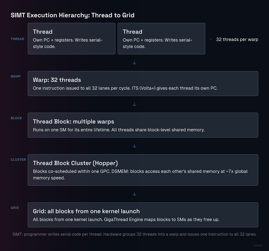
A thread is the unit of code a programmer writes. A warp is a group of 32 threads that the hardware executes together as the basic unit of scheduling. When a CUDA kernel launches, threads get partitioned into warps automatically, and from that point on, every instruction issue, every memory request, and every scheduling decision happens at warp granularity.
What ties the two granularities together is Single-Instruction, Multiple-Thread, or SIMT. SIMT differs from the older SIMD vector model in a way that matters for how kernels get written. SIMD requires the programmer to reason about vector width directly, packing data into vector registers and writing operations that act on the whole vector at once. SIMT lets the programmer write code as though each thread is independent, with its own variables and control flow, while the hardware groups threads into warps and issues one instruction to all 32 lanes at once. This is why CUDA kernels look like serial code with a thread index rather than hand-vectorized assembly.
Each thread inside a warp maintains its own program counter and its own slice of the register file. Hardware preserves the appearance of independent execution by tracking enough state per thread to support divergent control flow, but the issue rate is still one instruction per warp per cycle when all 32 threads are doing the same thing.
2.2 Independent Thread Scheduling
Pre-Volta GPUs ran warps in strict lockstep. A single program counter and a single call stack were shared across all 32 threads in a warp, and divergent branches were handled by an active mask that disabled threads not on the current path. This worked for straight-line numeric code but broke down when threads inside a warp tried to coordinate with each other through fine-grained synchronization. A thread holding a lock could be masked off while another thread in the same warp spun waiting for that lock to release, and the warp would deadlock because the masked thread never got to run.
Volta introduced Independent Thread Scheduling, or ITS, and Hopper carries it forward. Under ITS, hardware maintains per-thread program counters and per-thread call stacks. When threads in a warp diverge, a hardware schedule optimizer dynamically groups together the threads that are about to execute the same instruction and issues that instruction to them as a temporary SIMT unit while The remaining threads run on a separate cycle. SIMD-style throughput is preserved when threads agree on what to do next, and divergent cases are handled correctly without deadlocking on mutex-style patterns.
ITS does not eliminate the cost of divergence. A warp that splits down two different branches still serializes the work, and the cycles spent on each path are additive. What ITS provides is correctness for fine-grained synchronization patterns and a cleaner mental model where threads can be reasoned about as independent agents that happen to execute in groups when convenient.
2.3 The streaming multiprocessor on Hopper
A streaming multiprocessor, or SM, is the physical unit that runs warps. An H100 SXM5 contains 132 SMs, each one structurally identical, and the GigaThread Engine is the front-end scheduler that distributes thread blocks across them when a kernel launches. From that point on, each SM operates as an independent processor with its own warp pool, its own register file, and its own access to the L1 cache and shared memory.
Each H100 SM is partitioned into four sub-divisions, sometimes called quadrants or SMSPs. Every quadrant contains its own warp scheduler, its own dispatch unit, its own L0 instruction cache, and its own segment of the register file holding 16,384 32-bit registers. Across the four quadrants, an SM can hold up to 64 resident warps, which is 16 per quadrant. Each cycle, each quadrant’s scheduler picks one ready warp from its pool and issues an instruction to the appropriate execution unit.
Execution units inside each quadrant are specialized. Each quadrant has 32 FP32 CUDA cores, 16 INT32 cores, one special function unit for transcendentals like sin and log, and one fourth-generation Tensor Core that handles the matrix multiply-accumulate operations underlying nearly all modern deep learning. Dispatch units route each instruction to the right unit. A warp issuing an FMA goes to the FP32 cores, a warp issuing a matrix multiply goes to the Tensor Core, and these can happen in different quadrants on the same cycle.
L0 instruction caches are one of the more specific Hopper additions. Instruction fetch costs energy and latency, and on a chip with this many active warps, fetching the same instruction repeatedly from the SM-level L1 instruction cache adds up. Each L0 sits inside a quadrant and holds recently decoded instructions, so warps running tight inner loops fetch their instruction stream from a few hundred bytes away rather than from the shared SM cache.
2.4 Blocks, grids, and thread block clusters
Threads are grouped into thread blocks, also called Cooperative Thread Arrays, or CTAs, and a thread block is the level at which on-chip cooperation happens. Every block is guaranteed to execute on a single SM for its entire lifetime. This guarantee is what makes block-level shared memory possible, because all threads in the block are physically close to the same shared memory bank and can synchronize through hardware barriers without leaving the SM.
A grid is the collection of all thread blocks launched by a single kernel call. Grids can be enormous, often larger than the GPU itself, and the hardware schedules blocks onto SMs as SMs become available. Programmers specify grid and block dimensions at launch, and hardware handles the mapping.
Hopper adds a new level above the block, called the thread block cluster. A cluster is a group of thread blocks that the hardware guarantees will be co -scheduled on SMs within the same Graphics Processing Cluster, or GPC. As model and tile sizes grow, single-block shared memory is no longer enough, and pulling intermediate results through global memory to cooperate across SMs is expensive. Clusters expose Distributed Shared Memory, or DSMEM, which lets threads in one block load, store, and perform atomic operations directly on the shared memory of other blocks in the same cluster. According to NVIDIA’s Hopper architecture documentation, this SM-to-SM exchange runs about seven times faster than routing the same data through global memory. DSMEM extends the reach of cooperation from one SM to a small group of nearby SMs.
2.5 Occupancy and the resource budget
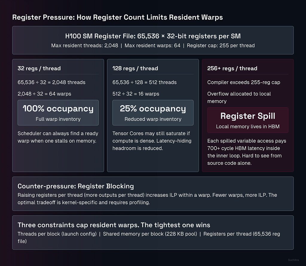
Occupancy is the ratio of resident warps on an SM to the maximum the SM can hold, which on the H100 is 64. Occupancy matters because the warp scheduler hides memory latency by switching to a different ready warp when the current one stalls, and it can only do that if there are enough warps resident to find one that is ready.
Three resources determine how many warps an SM can hold simultaneously. First is threads per block, which is set by the launch configuration. Second is shared memory per block, which competes for the SM’s 228 KB shared memory pool. Third is registers per thread, which competes for the SM’s 256 KB register file. A kernel that demands a lot of any of these reduces how many warps fit, and the most restrictive constraint wins.
Registers are the constraint that limits occupancy most often. An H100 register file holds 65,536 32-bit registers per SM. If a kernel uses 128 registers per thread, the SM can hold at most 65,536 / 128 = 512 threads, regardless of the 2,048-thread architectural ceiling. That works out to 16 resident warps and 25% occupancy. Tensor Cores might still be saturated by those 16 warps if the kernel is well-structured, but the headroom for hiding memory latency is gone, because the scheduler has fewer alternatives to switch to when a warp stalls on a load.
Hopper caps registers at 255 per thread. Going past this limit triggers register spilling, where the compiler stores excess variables in what CUDA calls local memory. Local memory is named misleadingly because it does not live anywhere local. It is allocated out of global memory, with the same 700-cycle access latency as any other HBM read. A kernel that spills registers heavily will see its inner loops slow by orders of magnitude, often without an obvious signal in the source code.
A counter-pressure complicates the occupancy story, which is register blocking. Increasing the work per thread, by having each thread process multiple output elements rather than one, raises register usage and lowers occupancy, but also increases instruction-level parallelism within a thread. A thread doing four independent FMAs in a row gives the hardware more flexibility to overlap arithmetic with memory access, and well-tuned kernels often deliberately accept lower occupancy to gain ILP. The right balance is workload-dependent and tends to require profiling to find.
2.6 Warp divergence
Warp divergence is the cost of the SIMT abstraction. When threads in a warp evaluate a branch condition differently and take different paths, hardware cannot issue both paths in a single cycle. It serializes the warp through both paths, masking off the threads not on the current path and running the active ones, then switching the mask and running the other group. A balanced 50–50 split through an if/else block doubles the effective execution time for that block.
Penalty is most visible in kernels with data-dependent control flow. A naive attention kernel that branches on whether a token is real or padding will pay divergence cost on every warp that straddles the boundary between the two. A naive sparse computation that branches on whether a value is zero will pay divergence cost whenever sparsity is irregular at warp granularity.
Production kernels handle this through warp specialization. Instead of letting threads inside a warp diverge, the kernel assigns entirely different roles to entirely different warps. FlashAttention-3, in the implementation described by Shah et al. in their 2024 paper, splits warps into producers and consumers, where producer warps fetch data from global memory while consumer warps run the attention math, and each warp internally executes a single coherent instruction stream. The producer-consumer split lets the kernel overlap memory transfers and compute without forcing a single warp to handle both, which keeps divergence at zero.
2.7 Little’s Law and the bridge to memory

Little’s Law gives the quantitative version of the latency-hiding argument. It states that for a stable system, the number of items in flight equals the throughput multiplied by the latency, or L = λ × W. Applied to a GPU, items in flight are active warps, throughput is the rate at which the SM completes operations, and latency is the time each operation takes to come back.
A concrete instance makes the implication clear. If memory loads from HBM take 400 cycles to complete on average, and the SM can issue one instruction per cycle, then keeping the SM busy requires at least 400 in-flight operations distributed across resident warps. If the kernel only has 100 active warps and each warp issues one outstanding load before stalling, the SM has 100 operations in flight and 300 cycles per loop where the execution units sit waiting for memory. Throughput collapses to a quarter of peak, regardless of how fast the Tensor Cores are.
Occupancy directly determines whether the latency-hiding mechanism has the inventory it needs to function. If a kernel cannot keep enough warps in flight to cover the actual memory latency of the operations it issues, the GPU operates in a latency-limited regime where the FLOPS rating on the spec sheet stops mattering. How much latency actually needs hiding is set by the memory hierarchy itself.
3. Where Data Lives
The latency that warps and occupancy exist to hide comes from a memory hierarchy with six tiers, each one orders of magnitude slower than the one above it. The cost of moving from one tier to the next is what determines whether a kernel runs well or poorly.

3.1 The hierarchy as a capacity-bandwidth-latency triangle
Every level of GPU memory trades three properties against each other. Capacity, bandwidth, and latency are the three dimensions. Closer to the SM means smaller and faster, and farther away means larger and slower. A well-written kernel keeps the working set as close to the SM as possible, and absorbs the cost when data has to come from farther away.
Six tiers are worth thinking about on the H100. Registers, the unified L1 cache and shared memory pool, the L2 cache, HBM3 global memory, NVLink for inter-GPU traffic, and off-chip storage like NVMe for systems that exceed the GPU’s HBM. Each tier is an order of magnitude or more slower than the one above it.
3.2 Registers
Registers sit at the top of the hierarchy with effectively one-cycle access and the highest aggregate bandwidth on the chip. Each H100 SM holds 256 KB of register storage, organized as 65,536 32-bit registers split across the four quadrants. Every thread carves out a private slice for its local variables, and the warp scheduler can read or write register operands in the same cycle that an instruction issues.
Register pressure is the primary cause of low occupancy, as Section 2.5 showed. A kernel using 128 registers per thread caps at 25% occupancy because the file does not have room for more concurrent threads. Pushing past 255 registers per thread triggers spilling into local memory, which sounds local but physically lives in HBM at 700-cycle latency. A kernel that spills hot variables in an inner loop pays that latency on every iteration, and the slowdown is often hard to see from the source code alone.
3.3 Shared memory and L1
Shared memory and L1 cache share a single 256 KB pool per SM, which the runtime partitions dynamically between the two roles. Up to 228 KB can go to shared memory, with the remainder serving as L1. Latency runs in the 30 to 40 cycle range, an order of magnitude slower than registers and an order of magnitude faster than HBM.
Shared memory is a programmer-managed scratchpad, and that property makes it useful for cooperation. A thread block can stage a tile of input data into shared memory once, and every thread in the block can then read that tile multiple times without going back to global memory. Tile-based GEMM kernels rely on this pattern. The kernel loads a slab of the input matrices into shared memory, all warps in the block compute against that slab, and only when the slab is exhausted does the kernel pull the next one from HBM. The reuse multiplier from staging is what lets matrix multiply run compute-bound on modern GPUs.
L1 acts as a coalescing layer for the same SM. When threads in a warp issue memory loads, the L1 cache groups requests from neighboring threads into the smallest possible number of memory transactions, which reduces pressure on the lower tiers. Coalesced access patterns, where thread i reads address base + i, run dramatically faster than strided patterns where each thread pulls a separate cache line.
3.4 L2 cache
L2 is the largest on-chip memory tier, 50 MB on the H100, and is shared across every SM on the GPU. Its job is to absorb the repeated reads of model weights that occur during inference. Once a weight tile lands in L2, every SM that needs it can pull it from there instead of returning to HBM.
Latency in L2 is not uniform, which is a detail most introductions skip. According to microbenchmarks of the Hopper architecture by Luo et al., published in 2025, an L2 hit close to the requesting SM costs around 258 cycles, while a far hit, where the requested line lives in a slice of L2 physically distant from the SM, can climb to roughly 743 cycles. L2 is partitioned across the chip, and the position of the cache slice relative to the requesting SM determines the access cost.
A miss in L2 forces a trip to HBM and pays the full off-chip latency. The 50 MB capacity matters because it sets the working-set threshold. If active weights and activations of a kernel fit in 50 MB, L2 absorbs nearly all the traffic. If they spill past it, every additional access drops into the slower tier below.
3.5 HBM3 global memory
HBM3 holds the model weights, the KV cache, and the activations that do not fit in any of the on-chip tiers. An H100 SXM5 ships with 80 GB of HBM3 across five active stacks, with peak bandwidth of 3.35 TB/s and access latencies that tend to fall in the high hundreds of cycles, often above 700.
Bandwidth at 3.35 TB/s is large in absolute terms and small relative to the demands of LLM decode. Reading a 70 billion parameter model in FP16 takes 140 GB of memory traffic per forward pass, and at 3.35 TB/s, the read alone takes about 42 milliseconds before any compute happens. Part two will return to this calculation with the roofline analysis that explains why bandwidth is the binding constraint for inference.
HBM3 is also where local memory lives, where register spills land, and where L2 evicts cold lines. Every miss in the upper tiers eventually converts into an HBM transaction, which is why kernels that thrash the cache hierarchy slow by orders of magnitude rather than by small constants.
3.6 NVLink
NVLink is the GPU-to-GPU layer, used when a model exceeds single-GPU memory and has to be sharded. Hopper supports 900 GB/s of NVLink bandwidth per GPU, with effective round-trip latencies in the low microseconds once protocol overhead is included.
NVLink matters for inference on models too large to fit in 80 GB, like a 70 billion parameter model in FP16, which needs at least two H100s for weights alone. Tensor parallelism splits each layer’s weight matrices across GPUs and uses NVLink to synchronize partial results between them. The 900 GB/s figure is fast in absolute terms, slower than HBM3, and becomes a bottleneck when communication patterns are frequent or fine-grained. Pipeline parallelism reduces this pressure by sending activations across GPUs once per layer rather than once per matrix multiply.
Multi-GPU communication is its own topic with its own optimization landscape, and the rest of this article stays on a single GPU. The point worth carrying forward is that the hierarchy does not stop at HBM. There is one more tier of bandwidth and latency cost when models cross the GPU boundary, and the cost of crossing it shapes how production systems are partitioned.
3.7 The asynchronous machine
Tensor Memory Accelerator, or TMA, is a Hopper-specific hardware unit that handles bulk asynchronous data copies between global memory and shared memory. Earlier architectures required threads to compute load addresses, issue load instructions, manage out-of-bound predication, and track completion manually. Every one of those tasks consumed registers and instruction slots that would otherwise go to compute.
TMA absorbs all of that into hardware. A kernel issues a single TMA instruction describing the source tensor, the destination shared memory address, the tile shape, and any boundary conditions, and the TMA engine handles the rest in the background while the SM continues running compute on previously loaded tiles. Threads that issued the copy do not wait for it. They wait on a barrier when they actually need the data, and in the meantime the warp scheduler runs other warps that have already received their tiles.
Two consequences fall out of this. First, registers freed from address arithmetic can be spent on compute, which lets kernels use larger tile sizes and improves arithmetic intensity. Second, data movement and compute can overlap cleanly, which is the practical realization of the latency-hiding model from Chapter 2. Little’s Law required enough in-flight operations to cover memory latency. TMA makes those in-flight operations cheap to launch, and the producer-consumer warp specialization pattern from FlashAttention-3 mentioned earlier is built directly on top of TMA on Hopper.
4. Where This Goes Next
The mental model from these three sections covers how a modern GPU is built. Throughput orientation drives the design at the silicon level. The SIMT execution model groups thousands of threads into warps that the SM scheduler can switch between . The six-tier memory hierarchy moves data from registers down to HBM and across NVLink, with the TMA engine making the upper transfers asynchronous. Occupancy, register pressure, and warp divergence are the levers that determine how well the latency-hiding machinery works in practice.
What this model does not yet explain is why LLM decode runs so far below the H100’s peak compute. Generating one token from a 70 billion parameter model means reading 140 GB of weights and performing about 140 billion operations on them. The ratio of operations to bytes loaded is what determines the runtime, and the ratio is set by the structure of decode itself, not by anything in the hardware that could be tuned away.
Part two builds the framework that makes this constraint precise. Arithmetic intensity, the roofline model, and the memory wall are the tools. LLM prefill and decode are the case study. By the end of part two, the runtime of decode will be derivable from the model size, the precision, and the memory bandwidth, and the architectural responses to the memory wall, KV cache management, quantization, and prefill-decode disaggregation, will follow as direct consequences of the framework.
Warps, Memory Hierarchy, and Why Bandwidth Beats FLOPS : How GPUs Actually Work, Part 1 was originally published in Towards AI on Medium, where people are continuing the conversation by highlighting and responding to this story.